با توجه به برگزاری «رویداد ملی ساخت تراشه میکروالکترومکانیکی (MEMS)»، خبرنگار روابط عمومی دانشگاه با دکتر علی خادمی، مدیر فنی اتاق تمیز میکرو/نانوفب آزمایشگاه مرکزی دانشگاه صنعتی شریف و دبیر این رویداد گفتگو کرد.
Given the event "National Event on Microelectromechanical Systems (MEMS) Chip Fabrication", a university public relations reporter interviewed Dr. Ali Khademi, the technical director of the Micro/Nanofab Cleanroom at Sharif University of Technology and the secretary of this event. Here is an excerpt from their conversation:
Dr. Khademi is a graduate of Sharif University of Technology with bachelor's and master's degrees. He obtained his PhD in Physics from the University of British Columbia in Canada. Afterward, he spent about 2 years as a postdoctoral researcher at the University of Victoria and then as a researcher at the National Research Council Canada (NRCC). Currently, he serves as an assistant professor in the Physics Department and the technical director of the Micro/Nanofab Cleanroom Laboratory at Sharif University of Technology.
Please explain what microfabrication is? In what areas does it work, and what are its general applications? What is its importance? How much global demand is there for this field?
Microfabrication or nanofabrication refers to the manufacturing processes carried out in microscale and nanoscale dimensions, where various processes are used to create structures or electronic and mechanical components in micrometer or nanometer dimensions. Examples include various microvalves, micropumps, microchannels, and micro or nanosensors. Manufacturing processes include methods like photolithography, wet and dry etching, and micromachining. These microstructures are fabricated by combining different materials on various substrates such as silicon, glass, or different polymers. These equipments find applications in various fields such as medicine, engineering, agriculture, environmental science, basic sciences, and more.
Systems fabricated in micro and nanoscale dimensions, referred to in engineering literature as Micro/Nano Electromechanical Systems (MEMS/NEMS), are a significant focus globally and have a large and growing market. According to forecasts, the market volume for these products is expected to exceed $22 billion by 2028.
To better understand the importance of this topic and the speed of growth in this market, consider this example: Oxford Nanopore Technologies raised £250 million from 2003 to 2014 to develop a microfluidic product. Last year, a Chinese company raised $300 million in just one year to develop a similar product and compete with Oxford Nanopore. This indicates intense competition in this field among developed countries, which is accelerating. Significant investments in infrastructure development needed for micro and nanoscale fabrication have been made in European countries like Switzerland and Belgium, as well as in countries like the United States, China, and Canada. As you can see, one of the important reasons for the differences between China and the United States in the Taiwan issue is that Taiwan is a producer of silicon, which is one of the most important materials used in micro and nanofabrication.
In Iran, work in the field of micro and nanofabrication is relatively new but gaining momentum. With the return of professors and experts who have conducted research and industrial work abroad in this area, there has been a positive trend emerging over the past few years. However, there is still much to be done.
Introduction to Cleanroom Concept:
What is a cleanroom? What happens in cleanrooms?
When manufacturing large-scale items such as cars or refrigerators, issues like dust contamination are negligible. However, when you aim to build devices on a micro and nanoscale, even particles whose dimensions are many times larger than the structures you're working on can become problematic. Therefore, manufacturing processes need to be carried out in a clean and isolated environment, where even the personnel wear special clothing or coverings to ensure the absence of any particulate matter.
Why is there a need for a centralized cleanroom?
At the university research level, the proper execution of research to achieve a product is heavily dependent on laboratory facilities and fabrication capabilities. Developing necessary infrastructure for fabrication is a prerequisite for producing knowledge-based products. Not only does producing competitive products for the global market require these facilities, but competition through process optimization and improving manufacturing quality is also possible. As we know, university professors always need suitable infrastructure for advanced projects. Previously in our country, it was common practice for professors to establish these infrastructures in their own or at most in specialized departmental laboratories. However, today due to interdisciplinary nature of advanced projects and high costs of equipment procurement and maintenance, providing these infrastructures for professors, especially for young professors and active research groups, has become problematic. The solution to overcoming this problem, which is implemented in all prominent universities worldwide, is the establishment of centers, workshops (manufacturing workshops).
The cost of constructing a cleanroom and the price of equipment used for micro and nano dimensions are both high. It is not feasible for each faculty member to have their own cleanroom within the university budget. Therefore, in all developed countries, the process is such that this investment is made once in a university to establish a centralized cleanroom with advanced equipment, so that all faculty members and students can benefit from its services.
In many countries around the world, this happens even on a national scale. For example, a large central cleanroom facility spanning several thousand square meters is established to serve all researchers of that country and even others. For instance, IMEC in Belgium has a central cleanroom facility of 12,000 square meters that provides international services.
On one hand, the gathering of knowledge, experience, and collaboration among researchers from various fields in a large central laboratory promotes networking, experience sharing, and accelerates the development of new technological products.
Please introduce the micro/nanofab cleanroom facility at Sharif University of Technology.
The field of micro and nano-scale component manufacturing technology is crucial and inseparable, continuing to grow and develop. Conducting research in this area, particularly investing in new avenues, accelerates the country's scientific progress towards nano and micro technologies. To this end, supported by the Presidential Deputy of Science and Technology and the Research Deputy, Sharif University of Technology established a cleanroom facility in 1401 (Gregorian calendar: 2022-2023) across two separate floors, totaling 240 square meters. This facility includes sections for manufacturing micro/nanometer devices and biological applications, currently ready to serve all researchers, students, and industries in this field.
The history of the cleanroom facility at Sharif University of Technology is distinctive. While similar facilities existed in the Electrical Engineering and Physics departments, none were fully active in both nano-scale and biological manufacturing services. Construction of this facility commenced in 1399 (Gregorian calendar: 2020-2021) and reached full operational capability by 1401 (Gregorian calendar: 2022-2023).
The micro/nanofab cleanroom at Sharif University of Technology is equipped with specialized facilities across different segments dedicated to nano or micro fabrication. A proper cleanroom structure necessitates an efficient ventilation system ensuring ideal temperature and humidity control. In the micro/nanofab cleanroom at Sharif University of Technology, a practical system known as hygienic HVAC air handlers is utilized. These systems are responsible for regulating temperature, humidity, air purification, and oxygen levels within the cleanroom. The cleanroom is equipped with three distinct layers of filtration, including HEPA filters, which purify incoming air through the HVAC system.
The cleanroom at Sharif University of Technology operates at both ISO Class 1000 and ISO Class 10000 standards. The lithography section operates at ISO Class 1000, while other sections operate at ISO Class 10000.
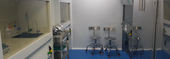
Entry into the cleanroom follows a strict protocol. Separate changing rooms designed with antistatic clothing are provided for men and women to minimize particulate and contamination entry, adhering to essential cleanliness standards.
The cleanroom facility is divided into several distinct zones, including:
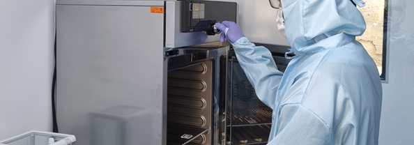
1- The PVD (Physical Vapor Deposition) section is dedicated to manufacturing microfluidic chips, equipped with an oven, a chemical hood, and a balance to facilitate operations in this field.
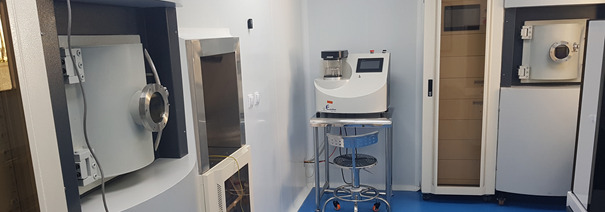
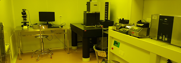
2- The Thin Film/ Dry Etching section includes deposition tools for coating conductors, insulators, semiconductors, and etching devices. Clusters and atoms of various materials are separated from crucibles and targets and deposited onto substrates ranging in size from millimeters to inches under high vacuum conditions. These thin films alter the optical, electrical, mechanical, and chemical properties of the substrates and, in some cases, embed micron-scale electrodes onto devices. The coating equipment includes a spin coater comprising both Direct Current (DC) and Radio Frequency (RF) sections. Another available deposition tool is the PVD device, which utilizes thermal evaporation and electron beam methods for vapor phase operations. Given the cleanroom's objective to support domestic production, these devices are sourced from local startup companies. Deposition processes necessitate optimal vacuum conditions; therefore, all equipment is equipped with turbo molecular pumps to achieve vacuum pressures of approximately 10-6 Torr. This setup offers advantages such as enhanced process speed, reduced contamination, and optimal parameter control during deposition processes. If we were to mention other equipment, there is an RIE (Reactive Ion Etching) machine in this section, operating in a plasma environment composed of reactive gas ions such as hydrogen, oxygen, SF6, for processes involving nano or micrometer scale etching or layer removal. Essentially, this machine performs surface micromachining to depths ranging from a few nanometers to several micrometers.
Additionally, for surface cleaning lasting a few minutes, an oxygen plasma device has been installed in the cleanroom. This device performs operations to remove contaminants, create hydrophilic conditions, and enhance reactivity.
Furthermore, the cleanroom also houses a fiber laser system with a power of 50 watts and a wavelength of 1064 nanometers for creating patterns, engraving, and marking on coated samples. This allows implementation of designs using specialized software.
3- The chemical fume hood section, covering an area of 10 square meters, is dedicated to handling and using chemical fluids and solvents. Necessary precautions have been taken for the proper storage of chemical substances. This section is equipped with locally manufactured hoods specifically designed for working with acids, bases, and solvents. To ensure safety during operations and prevent potential hazards, it is mandatory for personnel to wear acid-resistant gloves, aprons, safety goggles, and a full-face shield.An emergency shower is also installed in this section to allow immediate response in case of emergencies involving acids or hazardous chemicals, enabling the user to mitigate potential injuries promptly. All hoods are equipped with compressed air, pure water with a resistivity of 18.2 megaohm-centimeters, and auxiliary equipment such as a hot plate and magnetic stirrer.
4- The photolithography section covers an area of 14 square meters and operates at Class 1000 cleanliness level. It is designed for creating specific patterns and designs on thin layers or wafers in micrometer dimensions using photomasks, photoresist-sensitive materials, and a mask aligner machine with 1-micron precision. Photolithography is employed in this section to fabricate electronic components in micrometer dimensions with controlled designs.
Additionally, this section includes a dedicated workstation equipped with a spin coater for applying photoresist materials, a hot plate, and an ultrasonic bath. These tools enable users to work with solvents and materials necessary for their designs, particularly those involving photoresists and chemicals used in photolithography, which are sensitive to light.
5- The grey area is designed to prevent contamination from entering clean rooms due to equipment and pumps. Every effort has been made to ensure that all these devices have a single outlet so that contaminants are transferred outside the clean room and sections.
The Cleanroom Micro/Nanofab Facility at Sharif University of Technology operates under the Center For Lab Services supervised by the Vice Chancellor for Research. This facility provides specialized services in microfluidics and nanotechnology.
To access the services offered by the Cleanroom Micro/Nanofab Facility, individuals need to visit the central laboratory website and the cleanroom itself. Unfortunately, due to the lack of supportive policies, most domestic centers charge significantly higher fees for their services compared to higher-quality services offered in Europe. This practice runs counter to the promotion and development of such technologies. Conversely, top universities worldwide offer similar facilities at much lower costs, aiming to support relevant research. These centers benefit from substantial government support and reinvest their outputs into technology development, which serves as a backbone for economic advancement.
Despite these challenges, the Cleanroom Micro/Nanofab Facility at Sharif University strives to establish competitive pricing policies. By registering tests and services, the facility aims to support strategic technology initiatives for researchers, students, faculty, and industrial partners within the laboratory network
How would you evaluate the objectives and outlook of the Micro/Nanofabrication Cleanroom?
The current status of nanofabrication equipment in the country is not justified from any perspective. The recurring costs on equipment that are sometimes used only once a month in a laboratory, and the closure of laboratories to others due to personal interests, have led to unreasonable waste of national capital. The output of university cleanrooms, besides advancing research at the cutting edge of knowledge and technology, serves as a starting point and incubator for the growth and development of spin-off companies. For these reasons, the future objectives pursued by the Micro/Nanofabrication Cleanroom at Sharif University of Technology include training specialized human resources, providing specific support for research leading to knowledge-based products in nanotechnology, saving foreign exchange through offering micromachining services domestically rather than outsourcing, and providing recommendations and solutions for industrial challenges in sectors such as electronics, oil, energy, and aerospace. Given its features and current demand levels, the design, construction, and equipping of the second phase of this project, covering at least 1000 square meters for non-simultaneous use by 200 users, is imperative. Therefore, considering the national perspective governing the central cleanroom project at Sharif University of Technology and the pivotal role this center will play in the growth and development of knowledge-based products, and given the budget constraints and financial resources of the university, financing this project requires support from supra-university entities such as governmental agencies, including the esteemed Scientific Deputy of the Presidency, or private companies investing in university complexes. These entities aim to enhance the quality of products and meet their technological needs by strengthening the industry-university relationship.
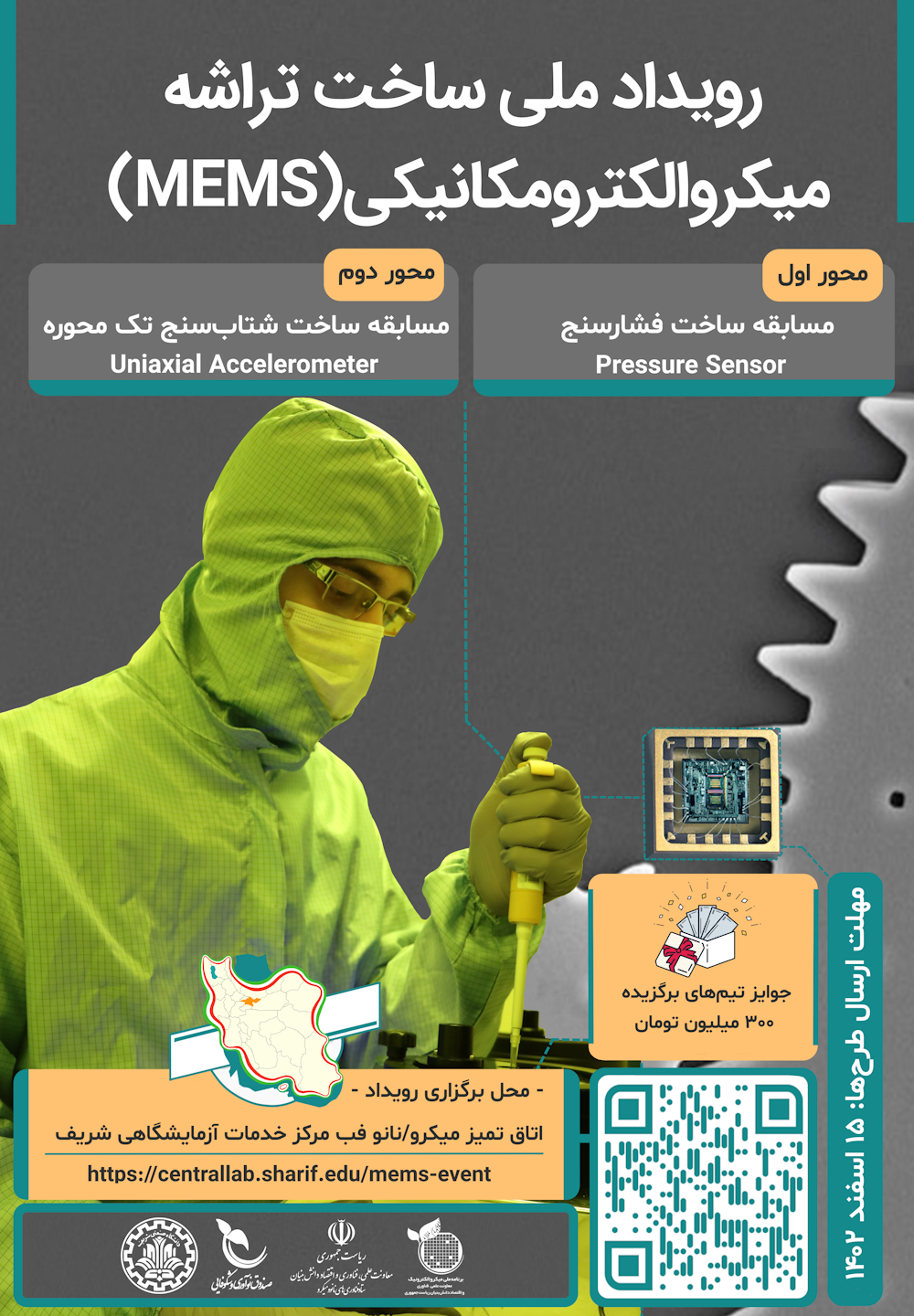
Please introduce the "National Microelectromechanical Systems (MEMS) Chip Manufacturing Event" and provide details about the topics, stages, prizes, supports, number of participants, and who can participate in this event.
This event, as one of the pioneering events in micro-scale manufacturing, is organized with the aim of familiarizing all professors, students, industry professionals, and active researchers in the field of micro and nano-scale manufacturing. It is supported by the Central Cleanroom Facility of Sharif University of Technology and the Vice Presidency for Science, Technology, and Innovation of the Presidential Office.
All individuals, regardless of their academic level, age, field of study, or profession, can participate in this event without any restrictions. One of the key objectives of this event is to gather all enthusiasts in this field together.
Participants compete in teams of 2 or 3 members in two topics: single-axis pressure sensor and accelerometer manufacturing.
Teams are required to present a proposal outlining the design and manufacturing process of their products at the outset. Proposals undergo initial evaluation before advancing to the next stage. The criterion for progressing to the next stage is the practical feasibility of the presented idea.
Selected teams can use the services of the Central Cleanroom Facility at Sharif University of Technology free of charge for manufacturing their products. Participation also includes access to training courses, free consulting services, and the opportunity to benefit from spiritual awards and honors from the National Elites Foundation.
The total prize pool for this event is 3 billion Iranian Rials, which will be awarded to the first and second place teams in each category (pressure sensor and accelerometer).
What are your plans for future events?
The feedback we receive from this event helps us plan and make decisions for future courses. However, this event marks the beginning of a long journey. We hope that in the coming years, we can invite students and professors from regional universities to witness the organization of a broader international event.
It is worth mentioning that soon a briefing session about this event will be held, and details will be announced shortly. Interested individuals are invited to register for updates and event announcements at the following link:
https://centrallab.sharif.edu/mems-event-pre-registration